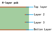
| Layer count |
1~32 layers |
The number of copper layers in the board. |
At present, ZXHPCB only accepts 1~32 layers of through-hole plates (buried blind-hole plates are not accepted) |
| Multilayer PCB Controlled Impedance |
4/6/8/10/12/14/16/18/20/.../32 layers |
Multilayer PCB support impedance design |
|
| Material |
FR-4 |
FR-4 Aluminum |
|
| The whole process |
Max. Dimension |
122cm*55cm |
Both sides can't be >55cm at the same time (one side can be 122.9cm, the other side
would have to be <55cm) |
| Soldermask Type |
Photosensitive ink(green,Blue,Red,Yellow,White,Black,Matte Black) |
Photopolymer inks are the most used type nowadays, and heat-set oils are generally
used in low-grade
single-sided cardboard. |
| Finished Outer Layer Copper |
1oz~3oz(35um~105um)
The default thickness of the outer layer of copper foil on
regular circuit boards is 1oz, up to 3oz. |
|
| Finished Inner Layer Copper |
0.5oz(17um)
Default conventional circuit board inner layer copper foil line thickness
is 0.5oz
|
| Board Thickness |
0.4 ~4.5 mm |
Thickness for FR4 are: 0.4/0.6/0.8/1.0/1.2/1.6/2.0/2.4/3.0/4.5mm (2.5 mm and above are for 12+ layer PCBs only) |
| Finished |
Board Thickness Tolerance |
Plate thickness ≧1.0mm, plate thickness tolerance ±10%.
Plate thickness <1.0mm, plate thickness tolerance ±0.1mm |
e.g. For the 1.6mm board thickness, the finished board thickness ranges from 1.44mm(T-1.6×10%) to 1.76mm(T+1.6×10%)
e.g. For the 0.8mm board thickness, the finished board thickness ranges from 0.7mm(T-0.1) to 0.9mm(T+0.1). |
| Multiple Printed Panel |
No gap splicing: 0 gap splicing
Gap splicing: 1.6mm gap splicing |
The gap of the spliced boards should not be less than 1.6mm, otherwise it is more
difficult to routing. |
| Multiple Printed Panel,V-cut Shipments |
Distance between wiring and solder pad to board edge: ≥ 0.4mm |
The line must be > 0.4mm spaced away from the edge, otherwise the V-cut will hurt
the line and the pads |
| Single piece shipments |
Distance between wiring and solder pad to board edge: ≥ 0.2mm |
Single piece shipments need to have ≥0.2mm spacing, otherwise the lines and pads
inside the board may be involved. |
| Drilled hole |
Drill/Hole Size(mechanical drilling) |
0.2~6.3mm |
Min. drill size is 0.2mm, Max. drill size is 6.3mm,
if greater than 6.3mm factory to be dealt with separately, mechanical drill
specifications for the 0.05mm for the first order, such as 0.25, 0.3mm |
| Hole Size Tolerance(Mechanical Drilling) |
±0.075mm |
Drilled holes with a tolerance of +/-0.075mm.
Eg. For the 0.6mm hole, the finished hole size between 0.52mm to 0.68mm is acceptable. |
| Minimum Borehole ID and OD |
Min.ID:0.2mm Mix.OD:0.45mm |
Multilayer PCB:Min.ID:0.2mm,Max.OD:0.45mm
Double Layer PCB:Min.ID:0.2mm,Max.OD:0.45mm
|
| Min Hole Size For Half-Hole Process |
≥0.65mm |
Half-hole process is a special process, the min. hole size shall not
<0.65mm,<0.65mm can not do the effect of half-hole |
| Through Hole Single Sideannular Ring |
5mil |
|
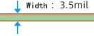
| Circuit |
Trace Width |
Single&Double Layer PCB,multilayer PCB are 3.5mil. |
 |
| Trace Spacing |
Single&Double Layer PCB,multilayer PCB are 4mil. |
 |
| Pad Edge To Wire Edge Spacing |
6mil |

|
| Min Character Width |
Conductor Width 4mil Character Height 27.5mil |

|
| Solder mask opening |
0.05mm |
If need solder mask bridge, it should be more than 4MIL.
Not to soldermask bridge as
the inspection and shipment standards. |
|
| Dimension Tolerance |
±0.15mm |
Board profile tolerance ±0.15mm |
|
| Min. Strips |
3mm |
|
|
| NOTE |
Pads Manufacturer Copper Layup Method |
Hatching |
|
| Outline |
Please use Outline to design if there are many non-plated (NPTH) holes. |
|
